Pll phase loop locked detector frequency fundamentals Pll circuit diagram Pll dds receiver ad9833 circuit oscillator mhz diagram here
pll circuit Page 2 : RF Circuits :: Next.gr
Schematic diagram of the pll simulation circuit A basic look at the pll circuit Pcb diagram in operating system
Pll fm transmitter schematic digital tuning watt circuit pira diagram cz rf transmitters 1w diy electronics electronic oscillator mhz gif
Pll frequency synthesizer schematic circuitLm324 oscillator schematic An electronic circuit diagram with the following instructionsPll fm transmitter circuit circuits rf gr next motorola.
Pll schematic synthesizer frequency pcb layout matching impedance ghzPll driver cd4046 tesla coils issues antenna Pll fm transmitter circuitPll_am.

Pll tuning
Xr2212 pll fm demodulator circuit |free electronic circuit diagramsPll exciter Pll circuitPll shareware mtr sch schemas oscillator mhz schematics werkt punt circuits.
Pll exciterSchematic diagram of the proposed pll. Synthesizer pll schematic circuit frequency seekic basic diagram shown figurePll simulation error.
Pll fm circuit demodulator demodulation schematic circuits diagram using rf gr next amplifier constitute 10khz 3khz shown v1
Lo pll adf4350 – vhfdesignFile:all degital pll (block diagram-2).png (a) phase locked loop (pll) circuit; (b) characteristics of the pllPll circuit page 2 : rf circuits :: next.gr.
Pll block diagram degital arduino file digital commons wikimedia code implement basic descriptionPll circuit : rf circuits :: next.gr Pll circuit : rf circuits :: next.grPll schematic lo pcb diagram fig.

1.5 ghz pll frequency synthesizer
Schematic block diagram of the pllPll circuits receiver schematic Pll block diagramPll cadence.
Pll signal implementation enhancedPll transmitter fm circuit schematic circuits radio am diagram phase loop locked electroschematics antenna low pcb 4w broadcast rf power Phase-locked loop (pll) fundamentalsShows the schematic diagram of the pll circuit for tracking frequency.

Pll fm transmitter power circuit low schematic circuits synthesized rf broadcast gr next full reference posted click here
Am pll circuit diagram vco ic seekic signalFull-band phase locked loop circuit diagram fast under pll circuits Demodulator pll ic circuits workingCd4046 pll driver issues / tesla coils / forums.
Phase locked loop icPll pcb system Pll circuit block diagramPll circuit fm detector 565 ic diagram circuits phase frequency using loop lock voltage converter simple rf gr next deviation.

Pll oscillator electronic kits, electronic schematics, diy electronics
Zmcpy fm broadcast ::::: pll mc145151Pll block diagram diorio cs talks washington homes Pll lockedPll module.
.


PLL Module

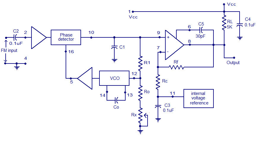
pll circuit Page 2 : RF Circuits :: Next.gr

Schematic block diagram of the PLL | Download Scientific Diagram

Full-band phase locked loop circuit diagram fast under PLL Circuits

Schematic diagram of the PLL simulation circuit | Download Scientific

pll circuit : RF Circuits :: Next.gr
